Finding a Debug Port
Removing the front panel light guide exposed something i was surprised i hadn’t seen somewhere else on the PCB; some test points for programming and / or debug purposes. With the help of a multi-meter and the reference manual I took a couple of minutes to find out what package pins the traces go to and if they had anything else connected to them. This would suggest the debug pins are reused after a boot and make things more difficult but, luckily, they weren’t.

Taking into account the possible I/O mux settings and the functions on the pins in this package there is !Reset, SWDIO and SWDCLK. That’s a little over what required to form a Serial Wire Debug (SWD) port as the reset line is extra but always helpful for putting the target into a known state. This port is presumably how the boards are programmed and checked in the factory since the production volume isn’t going to be high enough to entertain mask ROM based MCUs.
Building a Debug Probe
Now it’s known the MCU is ARM based and where a SWD port is probably available a way to connect to it is needed. Turns out the Raspberry Foundation created a firmware for the Pi Pico which turns it into a combined SWD probe and UART terminal for debugging another Pi Pico. There is even a driver for openOCD which allows it to use the Picoprobe (Pi Pico + Picoprobe firmware) as an interface. So, one firmware flash later and there’s the openOCD compatible SWD probe sorted.

The NXP website suggests the Kinetis part on the RKP is 5V only, and some probing of the RKP while powered up confirms this, so I’m going to need bidirectional level translation to connect to it. MOSFET level shifters are trivial to build but a parts order would be needed so premade ones save time and effort when they aren’t the goal of the project. These from Pololu (pictured above) and purchased through the Pi Hut will do the trick. They’ll accept 1.8-5 V on one side and 1.8-18 V on the other which is perfect for the debug port and, later, interfacing with the 12 V RKP bus.
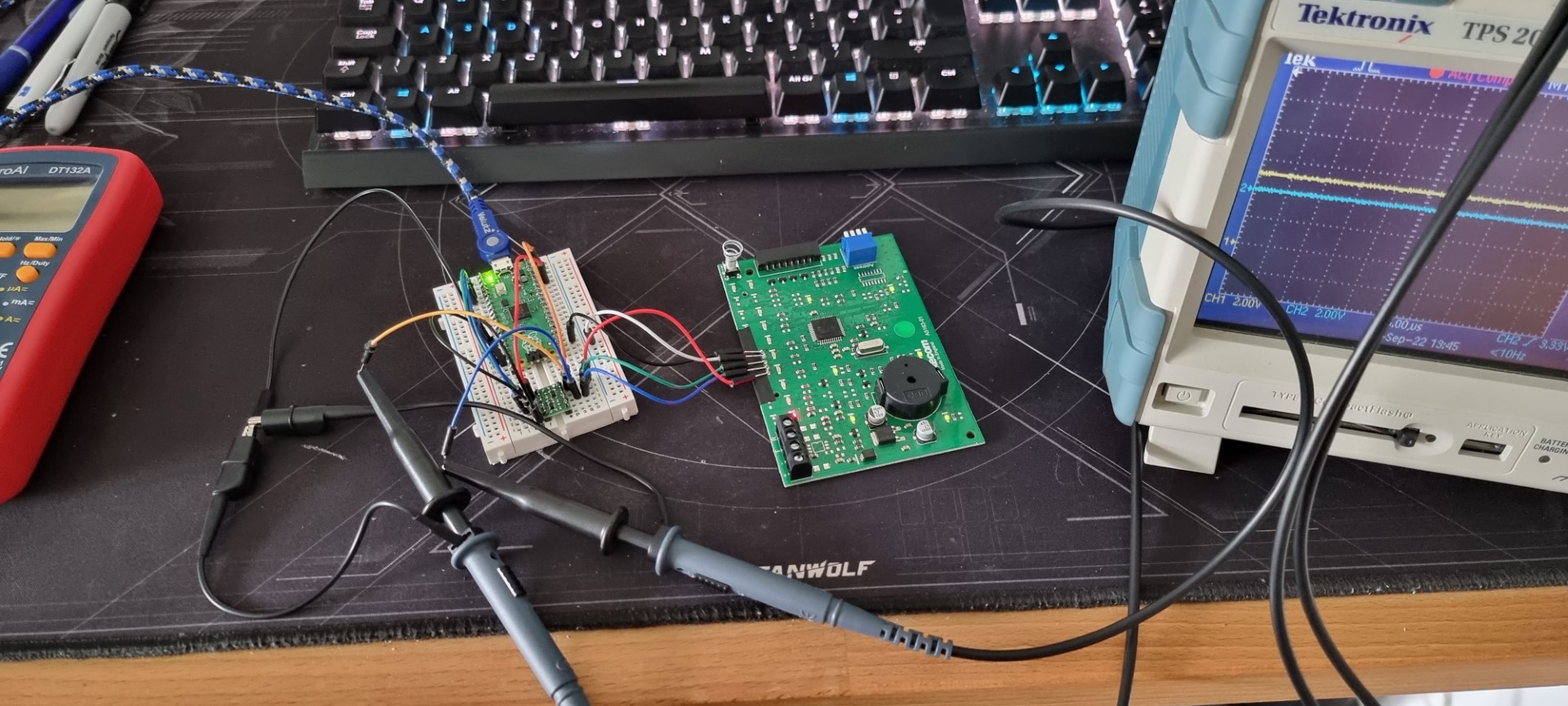
A jumpers and some breadboard later gives a tidy enough solution. The waveforms, not pictured, coming out of it look good enough even if the pull up to 5V from 3.3V is a bit slow.
Testing Connection
Building openOCD with the Picoprobe driver and finding the right configuration files for the interface and target took some time but it was all there built in since it’s common hardware.

It worked first time! (What do you mean? Of course I knew it would). Getting this far means we’re connected to the MCUs debug interface. In turn, this means the debug port isn’t disabled and the pins aren’t reused or remapped just to be awkward / practice good basic embedded security. I was expecting to have to (read: am slightly disappointed I don’t have to) build a voltage glitching rig to disrupt the portion of power up where data moved to the requisite register.
Poking at Flash
Now there’s a repeatable connection to the debug port we can have a look at the flash as check that’s accessible.

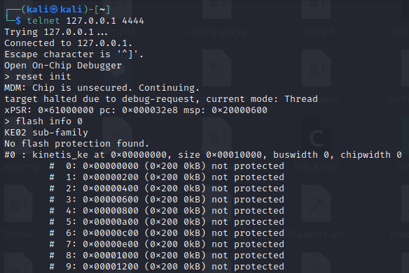
Being able to run “reset init” and have it complete is a good sign and furthermore it looks like all of the flash I’d expect (all upto 64 KB in a single bank) to be there is so the next step is to read out the flash and see if we get something sensible.
Stay tuned for Part 3!